Definition
Scanning electron microscope is a classification of electron microscope that uses raster scanning to produce the images of a specimen by scanning using a focused electron beam on the surface of the specimen.
- An SEM creates magnified images of the specimen by probing along a rectangular area of the specimen with a focused electron beam. This process is called the raster scanning.
- It is called a scanning electron microscope because the image is formed by scanning the surface of the specimen in a raster pattern using a focused electron beam.
- SEM relies on the secondary emission of electrons from the surface of the specimen to achieve magnified image to be viewed
- The major advantage of a SEM over TEM is that it can produce detailed image of the whole organisms and surfaces of the cells.
Working principle and Diagram of SEM
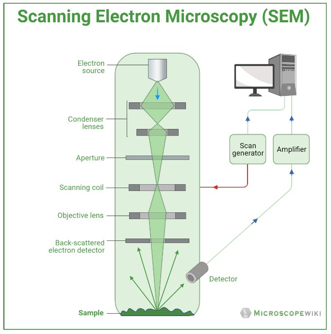
A scanning electron microscope works on the principle of targeting a focused beam of electrons moving with high kinetic energy on a specimen.
When these electrons scan the surface of the specimen, electrons are scattered and these secondary electrons that are slowed down on the impact of hitting the surface of the specimen are collected by a detector and these secondary electrons create the magnified image of the specimen thereby illustrating the morphology and topology of the specimen.
Similarly, the backscattered electrons from the surface of the specimen help us in illustrating the difference in composition of the specimen thereby making this type of microscope a useful instrument.
Difference between Transmission Electron Microscope (TEM) and Scanning Electron Microscope (SEM)

- The main difference between a transmission electron microscope (TEM) and scanning electron microscope is the fact that TEM operates by penetrating electrons through the specimen and producing image by capturing the emitted electrons from the specimen.
- On the other hand, SEM employs the technique of raster scanning the surface and capturing the secondary and back scattered electrons to create an image that illustrates the topology and morphology of the specimen and also plot the changes in composition using the back-scattered electrons.
Components (Parts)
The scanning electron microscope consists of the following major parts:
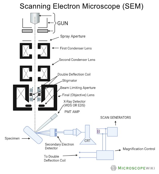
- Electron Gun
- Condenser Lens
- Objective Lens
- Sample stage
- Scanning Coil
- Detector
- Other infrastructure elements
- Power Supply
- Vacuum system
- Cooling system
- Area devoid of electric and magnetic fields
- Vibration-free floor
Electron Gun
- This is the basic part where the electrons are produced and directed towards the specimen for raster scanning.
- It contains a cathode and an anode and electrons are produced under thermal heat.
- The three types of electron sources that are used to generate a focused beam of electrons include : 1. Field emission gun (FEG), 2. Lanthanum hexaboride or a 3. Tungsten filament
Condenser Lens
- The condenser lens is used to adjust the amount of electrons that travel through the column to be focused on the specimen.
- The condenser can be used to increase or decrease the amount of electrons that are required to scan the surface of the specimen
Objective Lens
This lens is used to focus the beam of electrons onto the surface of the specimen
Sample Stage
- This is the area on which the sample is mounted.
- The sample stage can be moved up and down as per the requirement.
Scanning Coil
Also called as the deflection coil, the scanning coil is used to deflect the incoming beam of electrons onto the surface of the specimen.
Detector
- An SEM has several detectors that differentiate between the secondary electrons, back scattered electrons and diffracted electrons among others.
- These detectors help in creating the magnified image of the specimen
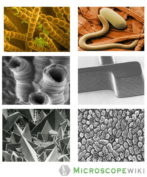
Applications
Scanning electron microscopes find great use in the fields of nanoscience studies, microbiology, and biomedical studies
- SEMs are used to analyze and study the very tiny filament structures of microorganisms
- They are used in analyzing the nanoscale ingredients that are used in cosmetic industry
- They are used to study the morphology and topology of elements used in various industries
- SEMs are used in spot analysis of chemical compositions in energy-Dispersive X-ray Spectroscopy.
Magnification Power of Scanning Electron Microscope
- The magnification of an SEM ranges from 10X to 3,000,000X
- The image magnification on SEM is not dependent on the power of the objective lens, as is the case with transmission electron and optical microscopes.
- Areas as tiny as 5 microns to approximately 1cm in width can be viewed using the scanning mode on an typical SEM
Advantages
- SEMs are robust, reliable and technologically advanced instruments
- They are user-friendly interfaces and trained users find it easy to operate
- Modern-day SEMs help in creating digital data of the specimen thereby making it easier to analyze it
- The SEMs are quick and the results are delivered fairly quickly, therefore aiding faster analysis of samples.
Disadvantages
- SEMs are very expensive and contains several sensitive components
- They are bulky and require several ancillary requirements to ensure proper function.
- They require special training to be handled
- They need special cooling systems, hence rendering their maintenance to be a hassle.
Prices of Scanning Electron Microscopes (SEM)
The type of electron microscope also decides the price of the microscope because of the various uses the microscope has and also on the components used in them.
The common types of electron microscopes that find widespread usage are Scanning Electron Microscopes (SEM), Focussed ion beam electron microscope (FIB) and Transmission Electron Microscope (TEM).
The table below gives you a fair bit of idea of prices about used as well as new electron microscopes. (Please note that the prices can be varied based on the vendor or offers in a given time. This information is to give a rough idea of the price in the market and also note that this is updated in September, 2022)
| Model | Type | Used Price | Estimated Price (New) |
| FEI Tecnai F20 | TEM | $395,000 | $592,500 |
| FEI Tecnai G2 F30 Twin | TEM | $395,000 | $592,500 |
| FEI Altura 810 | SEM | $350,000 | $525,000 |
| Philips CM 200F TWIN | TEM | $300,000 | $450,000 |
| FEI Tecnai 20 TWIN | TEM | $300,000 | $450,000 |
| Hitachi SU-70 | SEM | $275,000 | $412,500 |
| Hitachi 5500 | SEM | $250,000 | $375,000 |
| FEI Strata 210 | SEM | $250,000 | $375,000 |
| JEOL 1200ex II | TEM | $250,000 | $375,000 |
| FEI FIB 800-M | FIB | $250,000 | $375,000 |
| Hitachi 4700-II | SEM | $225,000 | $337,500 |
| FEI Tecnai 12 | TEM | $225,000 | $337,500 |
| FEI Quanta 200 | SEM | $200,000 | $300,000 |
| FEI FIB 200-S | FIB | $200,000 | $300,000 |
| Hitachi 5200 | SEM | $175,000 | $262,500 |
| Hitachi 4700-I | SEM | $175,000 | $262,500 |
| FEI CM200 | TEM | $175,000 | $262,500 |
| Philips CM 120 BT | TEM | $175,000 | $262,500 |
| FEI FIB 200-M | FIB | $175,000 | $262,500 |
| Philips CM12 | TEM | $161,000 | $241,500 |
| FEI XL40 | SEM | $155,000 | $232,500 |
| FEI XL30 | SEM | $150,000 | $225,000 |
| ZEISS EVO 50 | SEM | $150,000 | $225,000 |
| JEOL 1011 | TEM | $150,000 | $225,000 |
| Philips CM 120 | TEM | $150,000 | $225,000 |
| JEOL 1200ex I | TEM | $150,000 | $225,000 |
| JEOL JEM-2011 | TEM | $150,000 | $225,000 |
| Philips CM 100 | TEM | $150,000 | $225,000 |
| FEI FIB 200-P | FIB | $150,000 | $225,000 |
| FEI Morgagni | TEM | $135,000 | $202,500 |
| FEI Quanta 400 | SEM | $130,000 | $195,000 |
| Philips CM10 | TEM | $125,000 | $187,500 |
| Philips EM 208 | TEM | $125,000 | $187,500 |
| Hitachi 7000 | TEM | $105,000 | $157,500 |
| Zeiss EVO 40 | SEM | $95,000 | $142,500 |
| Hitachi 3000N | SEM | $85,000 | $127,500 |
Frequently Asked Questions
Q1. How many times can a scanning electron microscope magnify?
An SEM can magnify up to a million times (1,000,000x)
Q2. What can you see with a scanning electron microscope?
The SEM is typically used to create high-resolution images of shapes of objects and to show spatial variations in chemical compositions. They are used to understand the morphology and topology of the compositions of specimens
Q3. What is a Field emission scanning electron microscope?
Field emission scanning electron microscope (FE-SEM) is an advanced technology instrument that is used to capture the microstructure image of the materials.
Q4. Who discovered the scanning electron microscope?
Manfred von Ardenne developed the first version of the SEM in 1937
Q5. What is the cost of a scanning electron microscope?
The price of a new electron microscope ranges between $80,000 to $10,000,000 and above depending on the customizations, configurations, resolution, components, and brand value
References:
- https://www.sciencedirect.com/topics/neuroscience/scanning-electron-microscope
- https://en.wikipedia.org/wiki/Scanning_electron_microscope
- https://www.britannica.com/technology/scanning-electron-microscope
- https://www.biosciencenotes.com/scanning-electron-microscope-sem/
- https://serc.carleton.edu/research_education/geochemsheets/techniques/SEM.html
- https://tssmicroscopy.com/instruments/
- https://microscopeclarity.com/electron-microscope-cost/